Chapter 31 - Worked Solutions
to selected extension questions from the OUP text Senior Physics -
Concepts in Context by Walding,
Rapkins and Rossiter
Q2 :-
The diagram for the RLC circuit is as follows
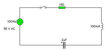
(a) resonance frequency FR = 1/2.p.(L.C)½ = 356 Hz.
(b) Effective current at resonance = VAC/R = 50/150 = 0.33A
(c) At resonance XC = XL = 2.23 x 10² W
Hence VC = VL = 0.33 x 2.23 x 102 = 73.5 V
Thus VR = 50V, VC = +74V, VL = -74V.
(d) Power P = V.I = 50 x 0.33 = 16.5 W
(e) Q-factor = 1/R.(L/C)½ = 1.5 using R, L and C values given.
Q9 :-
The combination of NAND gates produces the following "truth table" as compared to Fig. 31.18 in the text :-
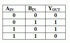
This appears to have no similarity to other gates in the main table of Fig.31.18
Q15 :-
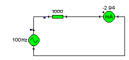
(a) Given a frequency f = 100 Hz and a resistor of 1000 W, the circuit would be as follows :-
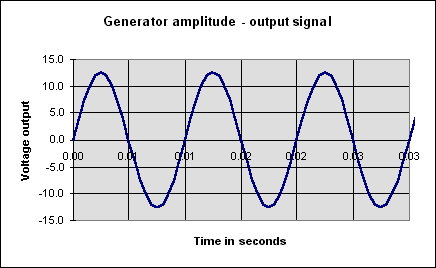
(b) The output waveform for 3 cycles would appear as :-
(c) Peak current IP = VP/R = 12/1000 = 12 mA.
Q18 :-
In circuit of Fig.31.30, C = 65 mF, VAC = 50 Hz @ 6.0 V
(a) XC = 1/(2.p.f.C) = 49 W while R = 15 W and
L = 22 mH, hence XL = 2.p.f.L = 6.9 W.
(b) Adding these values vectorially yields impedance ZAB = 48W, which when added to internal resistance of source gives total circuit impedance at f = 50 Hz of 53 W.
(c) IRMS = V/Z = 6/53 = 0.1 A.
(d) VAB = IRMS x ZAB = 4.2 V.
Q19 :-
Using the circuit diagram of Fig 31.31
(a) The simple rectifier is working as half-wave rectifier, providing smoothed positive and negative pulsed DC.
(b) The OP-Amp requires dual supply rails (±9V).
(c) The OP-Amp is amplifying the small induced voltage signal produced at it's no-inverting input.
(d) The variable resistor adjusts the amplifiers gain by adjusting feedback ratio.
(e) Probably to millivolts or microvolts AC.
Q21 :-
(a) Yes the supply would need to be regulated to allow the chip to operate without voltage fluctuations.
(b) There are 4 NAND gates on the 4011 chip.
(c) To allow the inputs to be taken High (+9V) or Low (0V) alternatively.
(d) To restrict the current draw by the LED's from the chip or supply rails.
(e) If InA1 pin1 is taken High by the flying lead, then 9V is applied to both the input pin and acts as a drive voltage for the LED which turns ON, showing pin InA1 is high. It is the same for the other input as well. When pin 3 goes High, a voltage is applied to the LED which turns ON. Truth Table is the same as a NAND gate in Fig. 31.18
(f) Yes this could be used with other single or Quad gate 40XX series chips.
 Return to Physics Textbook Home page